Packaging the die into a chip
14.1 · From wafer to a finished chip — flow
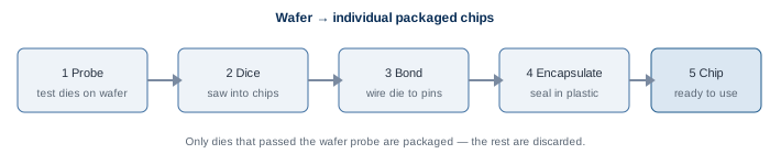
Section titled “14.1 · From wafer to a finished chip — flow”Back at the factory the finished wafer holds hundreds of dies, and packaging turns bare silicon into a handleable chip. Every die is first tested in place (probe), the wafer is sawn into individual dies (dice), each good die is wired to its package’s external contacts (bond), and finally sealed in protective plastic (encapsulate). Only dies that passed the wafer probe are packaged; the rest are discarded.
14.2 · Final test & speed binning
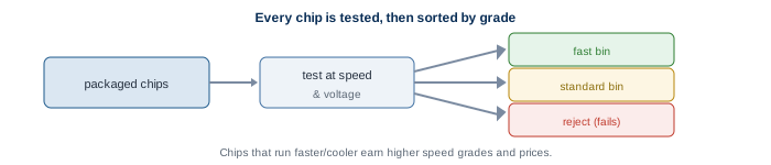
Section titled “14.2 · Final test & speed binning”Each packaged chip is then tested again at speed and voltage and sorted, or binned, by the grade it reliably meets: the fastest, coolest-running parts earn premium speed grades, ordinary parts go to the standard bin, and failures are scrapped. The output is one complete DRAM chip — but on its own it still cannot fill a CPU’s 64-bit bus.