The MOSFET switch
5.1 · Structure of an NMOS transistor
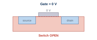
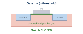
Section titled “5.1 · Structure of an NMOS transistor”The transistor is the star of the story: an electrically controlled switch with no moving parts. The modern version is the MOSFET. It is two N+ regions — the source and drain — in a P-type body, with a gate electrode over the gap, separated from the silicon by that thin SiO₂ gate oxide. The gate touches nothing electrically; it works purely through its electric field.

5.2 · OFF: gate at 0 V, no channel
Section titled “5.2 · OFF: gate at 0 V, no channel”With the gate at 0 V the switch is OFF. The only path from source to drain runs through back-to-back PN junctions that block current, so nothing flows — the switch is open.
5.3 · ON: gate above threshold builds a channel
Section titled “5.3 · ON: gate above threshold builds a channel”Raise the gate above a threshold voltage and the switch turns ON. The gate’s field pulls electrons up under the oxide, inverting a thin sliver of the P-body into a temporary N-type channel that bridges source and drain, and current flows. Because it is controlled by voltage rather than current, a MOSFET sips almost no power and switches in picoseconds — so it can be copied billions of times on one chip.
5.4 · Complementary pair: NMOS vs PMOS
Section titled “5.4 · Complementary pair: NMOS vs PMOS”MOSFETs come in a complementary pair. NMOS turns on when its gate is high (1); PMOS is the mirror image (P+ in an N body) that turns on when its gate is low (0). Having both available as opposites is exactly what makes the efficient CMOS logic of the next step possible.
