Synchronous & double data rate (SDRAM → DDR)
13.1 · SDR (one edge) vs. DDR (both edges)
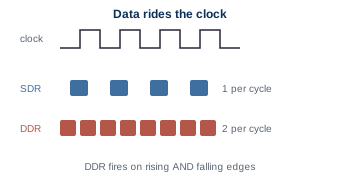
Section titled “13.1 · SDR (one edge) vs. DDR (both edges)”The arrays are static structures; this step is the protocol that makes them fast. Modern chips are SDRAM — Synchronous DRAM — tying every operation to a shared clock so memory and CPU stay in step. DDR (Double Data Rate) then sends data on both the rising and the falling edge of each clock cycle, doubling bandwidth without doubling the clock speed.
13.2 · Bursts, timing (CL·tRCD·tRP) & refresh
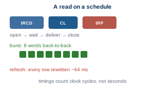
Section titled “13.2 · Bursts, timing (CL·tRCD·tRP) & refresh”Every access follows a fixed timing schedule, and the numbers on a RAM datasheet (like CL-tRCD-tRP) are simply cycle counts: tRCD is the activate-to-read delay, CL is the delay from the column command to data, tRP is the precharge time. Because opening a row is expensive, DRAM answers each request with a burst of several consecutive words, and a background refresh controller quietly rewrites every row roughly every 64 ms so no capacitor fades away.