The PN junction & diode
4.1 · A depletion region forms at the join
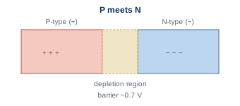
Section titled “4.1 · A depletion region forms at the join”Place a P-type region against an N-type region and something happens right at the boundary. Electrons and holes near the join recombine and cancel out, leaving a thin carrier-free depletion region of fixed charges. Those charges set up a built-in voltage barrier (~0.7 V) that opposes any further flow — this junction is the first real device.
4.2 · A diode: forward conducts, reverse blocks
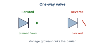
Section titled “4.2 · A diode: forward conducts, reverse blocks”That barrier makes the junction a diode, a one-way valve for current. Push voltage in the forward direction and it overcomes the barrier so current flows; push it in reverse and the depletion region widens and blocks it. The key insight is that a voltage can grow or shrink the barrier and thereby control conduction — precisely the trick the transistor exploits next.