Doping — N-type & P-type
3.1 · N-type: a Group V donor adds a free electron
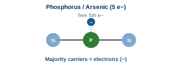
Section titled “3.1 · N-type: a Group V donor adds a free electron”Perfectly pure silicon is actually a poor, uncontrolled conductor. The breakthrough is doping: adding trace impurities to create spare carriers. Mix in a Group V element such as phosphorus or arsenic, which has five valence electrons — four bond into the lattice and the fifth roams free. These donor atoms make N-type silicon, whose majority (most abundant) carriers are negative electrons.
3.2 · P-type: a Group III acceptor adds a hole
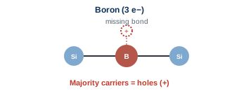
Section titled “3.2 · P-type: a Group III acceptor adds a hole”Do the opposite with a Group III element such as boron, which has only three valence electrons. One bond is left unfilled, leaving a hole that neighbouring electrons keep hopping into — so the hole effectively moves. These acceptor atoms make P-type silicon, whose majority carriers are positive holes. N-type and P-type are the two ‘inks’ we paint the crystal with.
3.3 · How little dopant, and the carrier vocabulary
Section titled “3.3 · How little dopant, and the carrier vocabulary”The amounts are astonishingly small — often about one dopant atom per hundred million silicon atoms — yet they change conductivity by orders of magnitude. A few terms carry forward: majority carriers are the abundant type, minority carriers the sparse opposite, and heavily doped regions are written N+ or P+. Everything electronic ahead is built from the boundaries between these regions.
