Refining & growing a wafer
2.1 · Purification — process flow (sand → 9N polysilicon)
Section titled “2.1 · Purification — process flow (sand → 9N polysilicon)”Raw sand is far too impure to build on, so silicon is first purified. Quartz sand (SiO₂) is reduced in a furnace to metallurgical-grade silicon (~99%), converted to a gas (trichlorosilane), distilled, and deposited back as ultra-pure polysilicon in the Siemens process. The target is ‘nine nines’ purity (99.9999999%) — fewer than one foreign atom per billion, because a single stray atom can ruin a transistor.

2.2 · Czochralski growth → the cylindrical boule
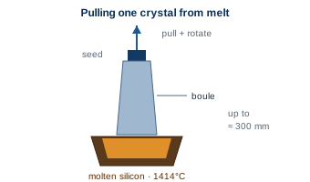
Section titled “2.2 · Czochralski growth → the cylindrical boule”Pure polysilicon is still a jumble of tiny crystal grains, but transistors need one continuous crystal. In the Czochralski process the silicon is melted at about 1414°C, a small seed crystal is dipped in, and it is slowly pulled upward while rotating. Melt atoms lock onto the seed’s orientation, growing a single flawless cylinder called a boule (or ingot), up to 300 mm across.
2.3 · Slicing & polishing into wafers
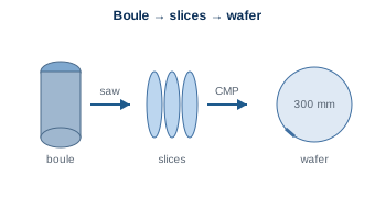
Section titled “2.3 · Slicing & polishing into wafers”The boule is sliced by a wire saw into thin discs called wafers, which are then polished by chemical-mechanical planarization (CMP) until they are flat to within a few atoms and mirror-smooth. This 300 mm wafer is the blank canvas — hundreds of identical chips will be built on it at once. From here on we can forget atoms and melts and simply treat the wafer as a perfect substrate.