Fabrication on the wafer
6.1 · The photolithography build cycle (repeats many times)
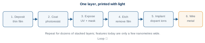
Section titled “6.1 · The photolithography build cycle (repeats many times)”Steps 3–5 describe what a transistor is; fabrication is how millions are printed on the wafer at once, photographically. A single layer is built by a repeating cycle: deposit a thin film, coat it with light-sensitive photoresist, expose it to UV through a patterned mask (photolithography), etch away the unwanted film, implant dopant ions to form the N+/P+ regions, and add metal wiring. This cycle repeats for dozens of stacked layers, with features only a few nanometres wide.
6.2 · Parallelism & yield: hundreds of dies per wafer
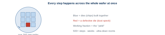
Section titled “6.2 · Parallelism & yield: hundreds of dies per wafer”Because every step happens across the whole wafer at the same time, hundreds of identical chips (dies) are made together. The full process can take 500+ steps over several weeks, in cleanrooms far purer than an operating theatre, since one dust speck can kill a die. The fraction of dies that work is called the yield; good ones are kept and defective ones discarded.